60 dB I & Q Vector ModulatorsFunctioning to simultaneously control the phase and amplitude characteristics in the processing of a microwave signal from 200 MHz to 22 GHz in up to 9:1 bandwidths. Narrowband models available from 22.0 GHz to 35.0 GHz with 10% bandwidth. Model offerings include digital or voltage controlled, low phase noise options, 500 ƞSec or 1.0 µSec switching speeds, and high dynamic range capabilities. |
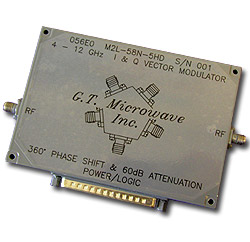 |
Description: The function of an I & Q Vector Modulator is to simultaneously control the phase and amplitude characteristics in the processing of a microwave signal. This vector modulator device will convert a signal to a desired vector location via a digital command.
Frequency Ranges: From 200 MHz to 22 GHz, up to 9:1 bandwidths available as well as any optimization. Narrowband models available from 22.0 GHz to 35.0 GHz with 10% bandwidth.
Operating Temperature Range: The 500 ƞSec models have an optional expanded operating temperature range from -55° to +85° C with a temperature coefficient of (±0.03 dB & ±0.10°)/° C. The 1.0 µSec models are better for temperature stability. Insertion phase drift is (0.03° x frequency)/° C or 0.1° min to 0.54° at 18 GHz. For severe environments, please consult the factory.
High Speed Switching: I & Q Vector Modulators listed are measured from any set value to any set value.
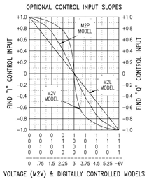
Digital or Voltage Controlled: I & Q Vector Modulators simultaneously control attenuation (dB) and phase shift (ø) by finding their I = 10 – (dB/20) cos ø & Q = 10 sin ø on the chart below and submitting the results to the Power/I & Q Logic connector.
Low DC Power Consumption: I & Q Vector Modulators require ±12 to ±15 VDC @ ±100 mA.
Stable Phase Shifts: Variation vs. temperature is typically ±0.17° & ±0.035 dB / degrees C from -10° to +65° for 500 ƞSec models. Slower models have better temperature coefficients, please consult the factory.
High RF Power Handling: For power levels greater than listed, please consult the factory.
Standard Interfaces: RF port connectors are ‘SMA’ female per MIL-C-39012. Please consult the factory for additional options.
Life Time Integrity: I & Q Vector Modulators can be designed to meet MIL-E-16400, Range 1 and MIL-E-5400, Class 2 environments operating within the -55° to +85° temperature range.
Low Phase Noise Option: Offers a typical performance of -132 dBc/Hz @ 10 kHz and -142 dBc/Hz @ 100 kHz offsets. Requires ±5 VDC (<2%) @ ±100 mA low noise regulated supplies and user supplied latch command for inputs. Please specify when ordering.
|
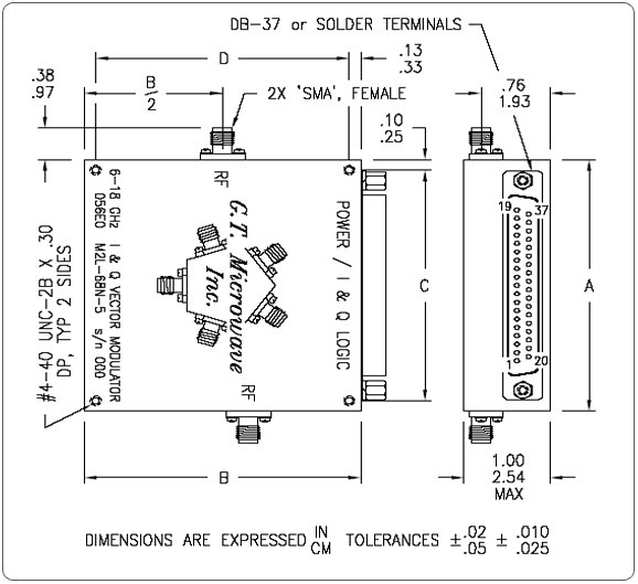
Outline Sizes |
||||
|
Size Reference |
‘A’ Dimension IN/CM |
‘B’ Dimension IN/CM |
‘C’ Dimension IN/CM |
‘D’ Dimension IN/CM |
|
1 |
4.95/12.57 |
3.38/8.58 |
4.75/12.07 |
3.13/7.94 |
|
2 |
5.55/14.10 |
3.25/8.26 |
5.25/13.34 |
3.05/7.75 |
|
3 |
4.75/12.07 |
3.25/8.26 |
4.50/11.43 |
3.00/7.62 |
|
4 |
3.25/8.26 |
3.00/7.62 |
3.00/7.62 |
2.75/6.99 |
Outline Diagram
For substantial improvement in performance, ask for optimized narrowband models.
|
Electrical Specifications for 500 ƞSec, 60 dB I & Q Vector Modulators |
||||||||
|
Model Number |
Frequency Range (GHz) |
Dynamic Range (dB/360°) |
Phase Error |
Amplitude Balance (dB) |
Insertion Loss (dB) |
VSWR |
RF Input Power CW/Max (dBm) |
Size Reference |
|
M2L-39A-5HD |
0.5-2.0 |
60 |
±15° |
±2.0 |
17.0 |
1.8:1 |
+5/+30 |
1 |
|
M2L-38A-5HD |
1.0-3.0 |
15.0 |
||||||
|
M2L-48A-5HD |
2.0-6.0 |
+10/+30 |
2 |
|||||
|
M2L-58A-5HD |
4.0-12.0 |
3 |
||||||
|
M2L-68A-5HD |
6.0-18.0 |
17.0 |
+15/+30 |
4 |
||||
|
M2L-84A-5HD |
16.0-22.0 |
50 |
2.0:1 |
|||||
|
Electrical Specifications for 1.0 µSec, 60 dB I & Q Vector Modulators |
||||||||
|
Model Number |
Frequency Range (GHz) |
Dynamic Range (dB/360°) |
Phase Error |
Amplitude Balance (dB) |
Insertion Loss (dB) |
VSWR |
RF Input Power CW/Max (dBm) |
Size Reference |
|
M2L-39A-1HD |
0.5-2.0 |
60 |
±15° |
±2.0 |
17.0 |
1.8:1 |
+15/+30 |
1 |
|
M2L-38A-1HD |
1.0-3.0 |
15.0 |
||||||
|
M2L-48A-1HD |
2.0-6.0 |
+23/+30 |
2 |
|||||
|
M2L-58A-1HD |
4.0-12.0 |
3 |
||||||
|
M2L-68A-1HD |
6.0-18.0 |
17.0 |
+25/+30 |
4 |
||||
|
M2L-84A-1HD |
16.0-22.0 |
50 |
2.0:1 |
|||||
|
Power/Logic Connections |
|||
|
PIN |
Function |
PIN |
Function |
|
1 |
I – 5 |
20 |
I – 4 |
|
2 |
I – 6 |
21 |
I – 7 |
|
3 |
I – 8 |
22 |
I – 3 |
|
4 |
I – 9 |
23 |
I – 2 |
|
5 |
I – 10 |
24 |
I – 1 (LSB) |
|
6 |
I – 11 |
25 |
I – 12 (MSB) |
|
7 |
No Connection |
26 |
No Connection |
|
8 |
+15 V / 150 mA |
27 |
No Connection |
|
9 |
Ground |
28 |
No Connection |
|
10 |
Ground |
29 |
No Connection |
|
11 |
-15 V / 150 mA |
30 |
No Connection |
|
12 |
Q – 3 |
31 |
No Connection |
|
13 |
Q – 2 |
32 |
Q – 4 |
|
14 |
Q – 1 (LSB) |
33 |
No Connection |
|
15 |
Q – 5 |
34 |
No Connection |
|
16 |
Q – 6 |
35 |
Q – 12 (MSB) |
|
17 |
Q – 7 |
36 |
Q – 11 |
|
18 |
Q – 8 |
37 |
Q - 10 |
|
19 |
Q - 9 |
|
|
|
All unused PINs have no internal connections |
|||